Control of electron flow and magnetism in atomically thin metal oxides
By Alexander Boris and Bernhard Keimer
In modern microelectronic devices, electrons flow in channels that are beginning to approach atomic dimensions. Because the heat they generate degrades the delicate atomic structures and hampers device operation, the current semiconductor-based technology is approaching fundamental limitations. Researchers are therefore looking beyond semiconductors and are beginning to explore more complex materials as potential device platforms. A particular focus has been on metal-oxide compounds, which show a much greater variety of properties than semiconductors and thus promise entirely new functionalities. Electrons in some metal oxides form a superconducting state in which they conduct electricity without generating any heat at all. In others, they form magnetically ordered states that are useful for information storage. Current research on metal oxides aims to predict and manipulate the formation of these states in a controlled and reliable fashion.
Investigating metal-oxide layers
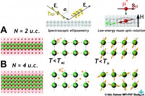
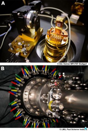
Together with an international team of researchers, we have now taken an important step in this direction. The team built devices out of thin layers of two different metal oxides, which are metallic and insulating in bulk form (Fig. 1). When the layers are more than three atomic monolayers thick, the electrons behave in a manner closely similar to the one in the bulk. In devices where the conduction electrons are confined to two atomic monolayers separated by insulating layers, their behavior changes completely. Upon cooling the device, optical reflection experiments with synchrotron radiation (Fig. 2A) revealed that they first form an insulating state in which every electron is attached to a particular atomic site, such that current flow is inhibited. Upon further cooling, the magnetic moments of these localized electrons then arrange in a regular pattern with neighboring moments antiparallel. As opposed to ferromagnetism, where all moments point in the same direction, this form of magnetic order is termed “antiferromagnetism”. The collective behavior of the electron system in these metal-oxide devices can thus be accurately controlled by adding a single atomic monolayer.
Using muons to detect magnetic order
To detect antiferromagnetic order in the atomically thin layers we required a novel, highly sensitive experimental method. Unlike ferromagnets, where the microscopic magnetic moments of the electrons add up to a macroscopically detectable magnetization, the electronic moments in antiferromagnets cancel out and are therefore invisible to ordinary experimental probes. We applied a method in which microscopic magnetic field sensors are implanted into the device. Since the sensors should not disturb the atomic structures they are intended to explore, they must be smaller than atoms – a requirement that can only be satisfied by elementary particles. Muons, which are in many ways similar to electrons but carry a much smaller magnetic moment, are ideal for this purpose. The muons are produced in particle accelerators and have to be slowed down such that they come to rest in the thin atomic device rather than blasting through it – a feat that we accomplished recently at the Low Energy Muon beamline of the Paul Scherrer Institute in Villigen, Switzerland, thanks to support by NMI3 (Fig. 2B). Muons are unstable and decay only two microseconds after they are implanted into the device. The decay products, positrons, are stable particles that are propelled out of the device, where they can be picked up in a detector. The direction of the positron beam then contains incisive information about the alignment of electron magnetic moments close to the parent muons in the device.
Original Publication:
A. V. Boris, Y. Matiks, E. Benckiser, A. Frano, P. Popovich, V. Hinkov, P. Wochner, M. Castro-Colin, E. Detemple, V. K. Malik, C. Bernhard, T. Prokscha, A. Suter, Z. Salman, E. Morenzoni, G. Cristiani, H.-U. Habermeier, and B. Keimer, “Dimensionality Control of Electronic Phase Transitions in Nickel-Oxide Superlattices”, Science 332, 937 (2011).
Dr. Alexander Boris is senior scientist and Professor Bernhard Keimer is director at the Max-Planck Institut für Festkörperforschung in Stuttgart, Germany.


